In today’s post, I design an SOIC-to-DIP adapter PCB in KiCAD!
Background
Circuit components can be sold in a number of different packages. Hitherto, for prototyping, I’ve used DIP packages (Dual In-Line), which are through-hole mounted and easy to use with a breadboard.
However, many components are only available in surface-mount versions, which can’t be used with a breadboard. For my prototyping purposes, I want to adapt these to through-hole format, which means I need an adapter PCB.
I cooooooould have bought four of them for $3.75, but the cost of small PCB manufacturing through a vendor like Oshpark is small enough for me to justify the practice.
Software
- KiCAD, the leading open-source professional PCB design software.
Design/Constraints
I’m using the STM32C011J6M6 microcontroller (datasheet link, PDF), which comes in an SOIC format with the following pinout:
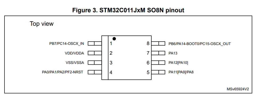
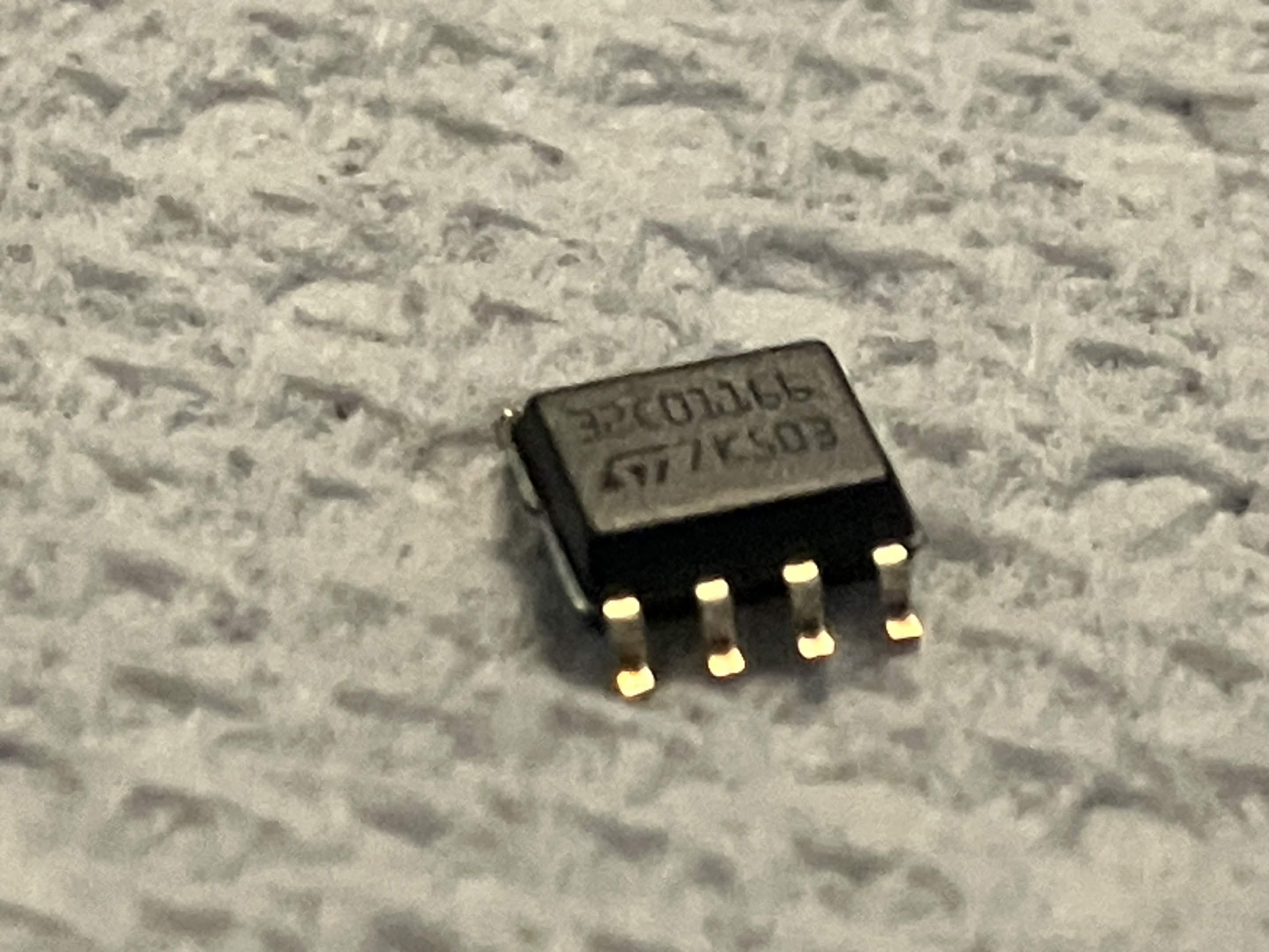
As you can see, in lieu of the usual corner “dot”, the component has a sloped ridge on one side to help with orientation.
I want to adapt this to a through-hole mounted format so that I can use it with a breadboard.
Process
I recommend the official KiCAD Getting Started Tutorial for additional detail on each step. This post is only a high-level overview of the process.
Starting the schematic
Once you’re in KiCAD, open the schematic editor and “Add Component” to add the microcontroller and a couple of headers:
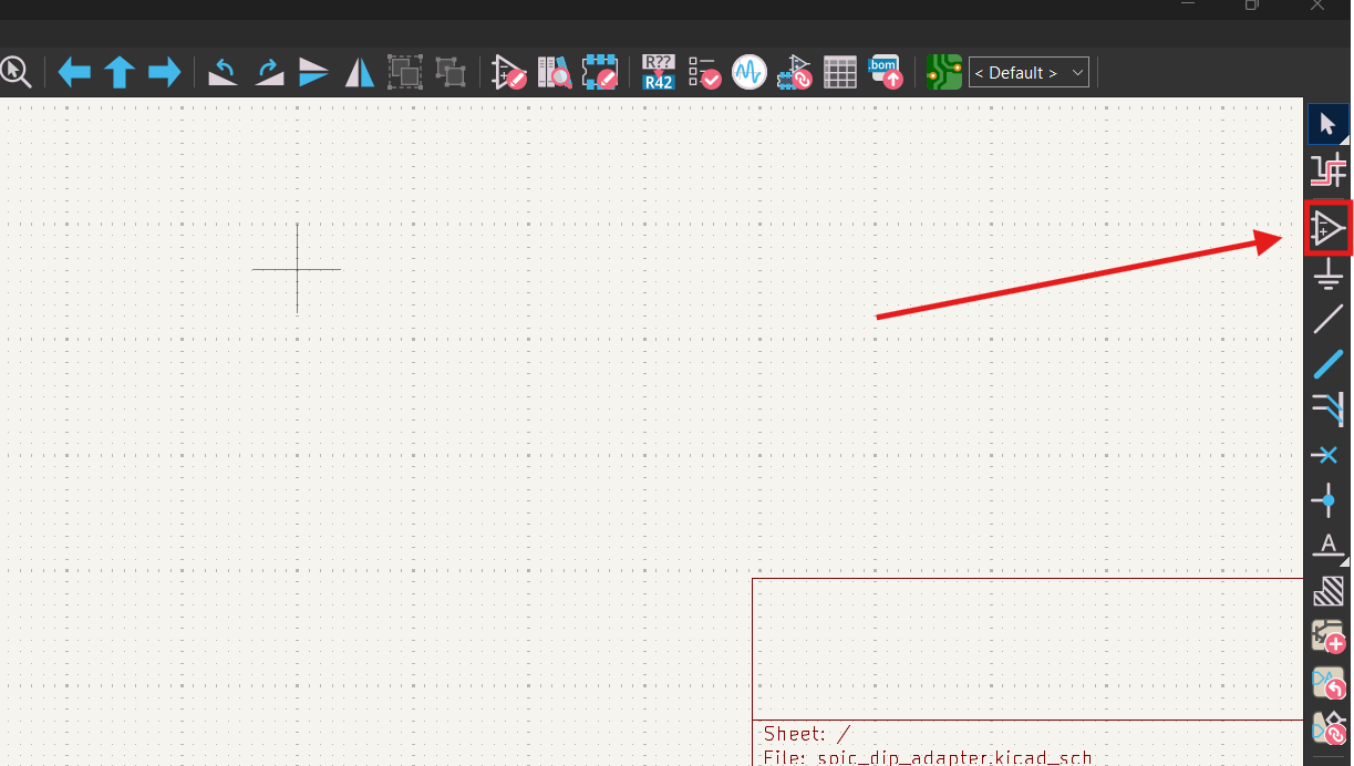
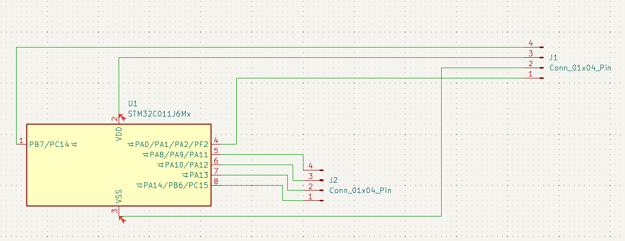
Make sure to run the Electrical Rules Check (ERC) to catch any flagrant issues:
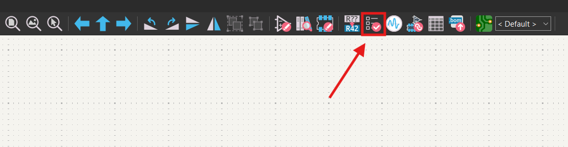
In this case, it warned me about not connecting any power or ground to the respective pins, which is fine - we’re just building an adapter.
Selecting footprints
Footprints represent the physical layout of the component, which is absolutely critical for PCB manufacturing.
The microchip already had a suitable footprint (or so I thought at the time), so I only needed to adjust the header footprint. I selected a 2.54mm-spaced pin header footprint, which is a tenth of an inch; standard breadboard hole spacing in the US.
Arranging the PCB
The next step is to arrange our schematic into an actual PCB. Follow the KiCAD Tutorial again to open the PCB editor and import changes from the schematic:
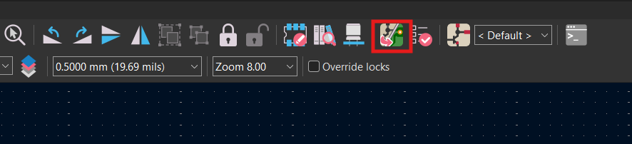
Lay out the components, drawing traces between them:
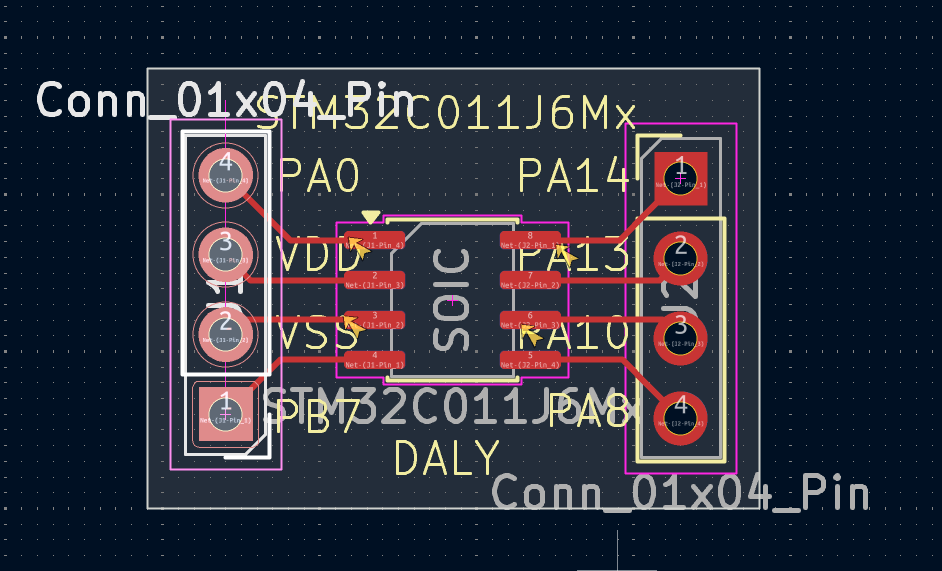
I also added a silkscreen (the cool professional-looking white text) on top with my notional pinout.
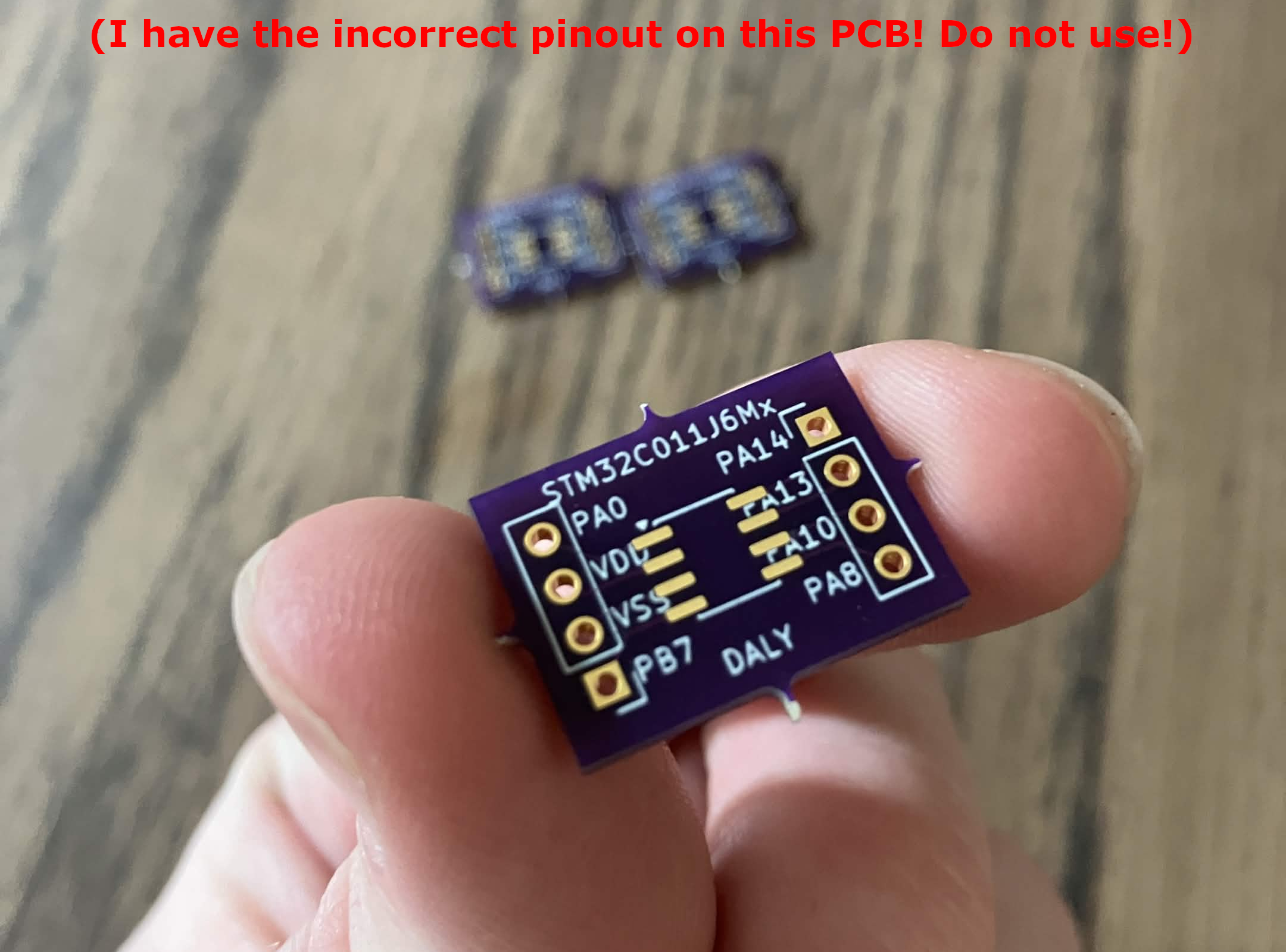
By this time, you may have realized that my STM32 footprint doesn’t exactly match the datasheet. This is something I didn’t catch until after ordering, and I have to live with an inaccurate silkscreen now :)
Finally, run the Design Rules Check (DRC), and, barring any warnings, you’re done!
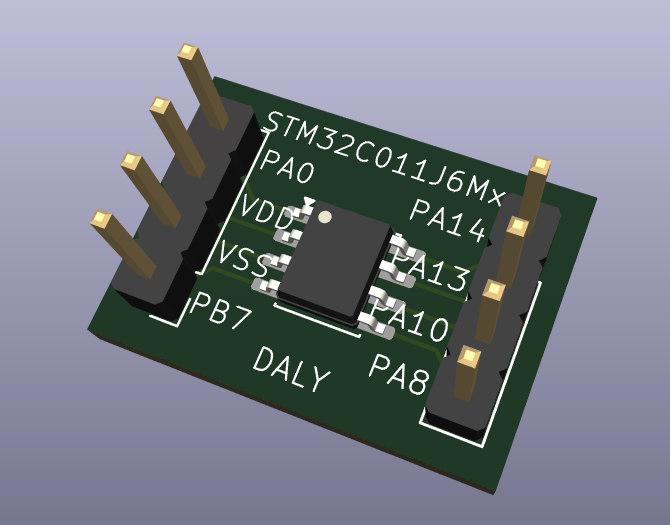
Ordering
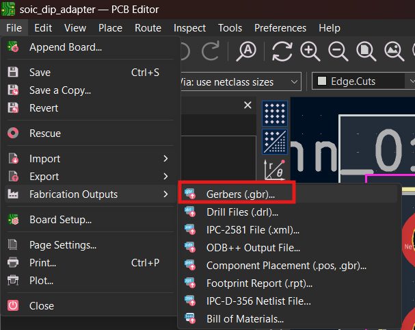
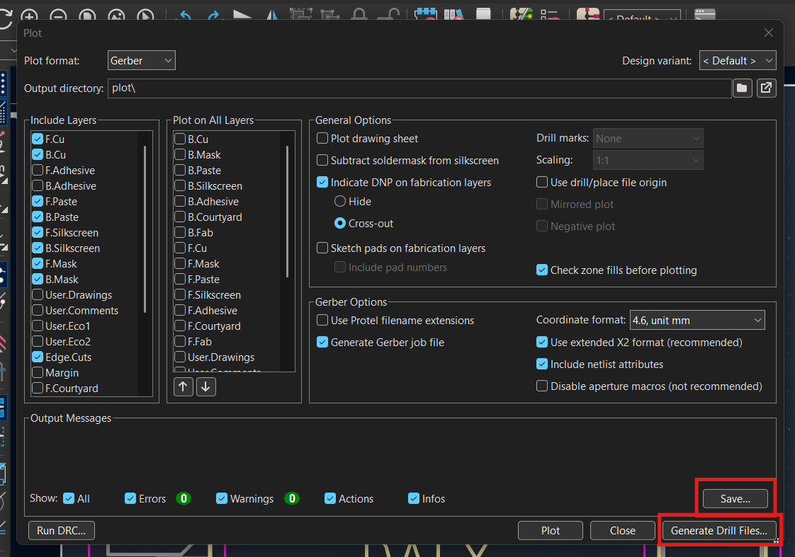
I ordered from Oshpark, which charged me $2.10 for three PCBs with free shipping. Oshpark accepts KiCAD files natively, but other PCB manufacturers may not. In those cases, you need to export both the Gerber files (which cover most of the routing and actual PCB design) and the drill files (which cover where to… drill):
12 days after ordering, my PCBs arrived, in suitable fashion! The parts jutting out are an artifact from how the PCB was laid out for fabrication; many manufacturers let you pay extra for deburring (or you can do it yourself).
Next steps
My PCB design could certainly be improved by:
- Double-checking the datasheet to ensure the silkscreen is accurate
- Checking the distance between the two sets of headers to ensure it fits on a breadboard (I got lucky)
Thanks for reading!